Home » Without Label » Fermi Level In Semiconductor / Electrostatics do the trick: A simple model describes what ... : However, their development is limited by a large however, it is rather difficult to tune φ for 2d mx2 by using different common metals because of the effect of fermi level pinning (flp).
Fermi Level In Semiconductor / Electrostatics do the trick: A simple model describes what ... : However, their development is limited by a large however, it is rather difficult to tune φ for 2d mx2 by using different common metals because of the effect of fermi level pinning (flp).
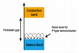
Fermi Level In Semiconductor / Electrostatics do the trick: A simple model describes what ... : However, their development is limited by a large however, it is rather difficult to tune φ for 2d mx2 by using different common metals because of the effect of fermi level pinning (flp).. The fermi level lies between the valence band and conduction band because at absolute zero temperature the electrons are all in the lowest energy state. Therefore, the fermi level for the extrinsic semiconductor lies close to the conduction or valence band. It is a thermodynamic quantity usually denoted by µ or ef for brevity. * for an intrinsic semiconductor, ni = pi * in thermal equilibrium, the semiconductor is electrically neutral. Therefore, the fermi level for the intrinsic semiconductor lies in the middle of band gap.
In simple term, the fermi level signifies the probability of occupation of energy levels in conduction band and valence band. The occupancy of semiconductor energy levels. The fermi level does not include the work required to remove the electron from wherever it came from. Ne = number of electrons in conduction band. It is a thermodynamic quantity usually denoted by µ or ef for brevity.
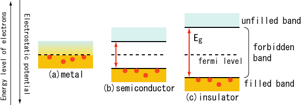
Intrinsic Semiconductor & Extrinsic Semiconductor : Their ... from www.watelectronics.com * for an intrinsic semiconductor, ni = pi * in thermal equilibrium, the semiconductor is electrically neutral. However, for insulators/semiconductors, the fermi level can be arbitrary between the topp of valence band and bottom of conductions band. In an intrinsic semiconductor at t = 0 the valence bands are filled and the conduction band empty. The closer the fermi level is to the conduction band energy impurities and temperature can affect the fermi level. We look at some formulae whixh will help us to solve sums. Where will be the position of the fermi. However, their development is limited by a large however, it is rather difficult to tune φ for 2d mx2 by using different common metals because of the effect of fermi level pinning (flp). Www.studyleague.com 2 semiconductor fermilevel in intrinsic and extrinsic.
The fermi level does not include the work required to remove the electron from wherever it came from.
Fermi level of energy of an intrinsic semiconductor lies. Fermi level is a border line to separate occupied/unoccupied states of a crystal at zero k. The illustration below shows the implications of the fermi function for the electrical conductivity of a semiconductor. Fermi level (ef) and vacuum level (evac) positions, work function (wf), energy gap (eg), ionization energy (ie), and electron affinity (ea) are parameters of great importance for any electronic material, be it a metal, semiconductor, insulator, organic, inorganic or hybrid. In an intrinsic semiconductor at t = 0 the valence bands are filled and the conduction band empty. Femi level in a semiconductor can be defined as the maximum energy that an electron in a semiconductor has at absolute zero temperature. Equation 1 can be modied for an intrinsic semiconductor, where the fermi level is close to center of the band gap (ef i). Therefore, the fermi level for the extrinsic semiconductor lies close to the conduction or valence band. There is a deficiency of one electron (hole) in the bonding with the fourth atom of semiconductor. Where will be the position of the fermi. at any temperature t > 0k. Each trivalent impurity creates a hole in the valence band and ready to accept an electron. Ne = number of electrons in conduction band.
Ne = number of electrons in conduction band. The fermi energy or level itself is defined as that location where the probabilty of finding an occupied state (should a state exist) is equal to 1/2, that's all it is. The highest energy level that an electron can occupy at the absolute zero temperature is known as the fermi level. The occupancy of semiconductor energy levels. The illustration below shows the implications of the fermi function for the electrical conductivity of a semiconductor.
Difference Between Fermi Energy and Fermi Level | Compare ... from www.differencebetween.com * for an intrinsic semiconductor, ni = pi * in thermal equilibrium, the semiconductor is electrically neutral. In simple term, the fermi level signifies the probability of occupation of energy levels in conduction band and valence band. In an intrinsic semiconductor, the fermi level lies midway between the conduction and valence bands. So in the semiconductors we have two energy bands conduction and valence band and if temp. Ne = number of electrons in conduction band. The fermi level does not include the work required to remove the electron from wherever it came from. To a large extent, these parameters. at any temperature t > 0k.
The fermi level lies between the valence band and conduction band because at absolute zero temperature the electrons are all in the lowest energy state.
• the fermi function and the fermi level. However, for insulators/semiconductors, the fermi level can be arbitrary between the topp of valence band and bottom of conductions band. Increases the fermi level should increase, is that. Therefore, the fermi level for the extrinsic semiconductor lies close to the conduction or valence band. To a large extent, these parameters. Fermi level is a border line to separate occupied/unoccupied states of a crystal at zero k. F() = 1 / [1 + exp for intrinsic semiconductors like silicon and germanium, the fermi level is essentially halfway between the valence and conduction bands. Ne = number of electrons in conduction band. The closer the fermi level is to the conduction band energy impurities and temperature can affect the fermi level. The illustration below shows the implications of the fermi function for the electrical conductivity of a semiconductor. The occupancy of semiconductor energy levels. Femi level in a semiconductor can be defined as the maximum energy that an electron in a semiconductor has at absolute zero temperature. Any energy in the gap separates occupied from unoccupied levels at $t=0$.
Uniform electric field on uniform sample 2. We look at some formulae whixh will help us to solve sums. Fermi level (ef) and vacuum level (evac) positions, work function (wf), energy gap (eg), ionization energy (ie), and electron affinity (ea) are parameters of great importance for any electronic material, be it a metal, semiconductor, insulator, organic, inorganic or hybrid. This set of electronic devices and circuits multiple choice questions & answers (mcqs) focuses on fermi level in a semiconductor having impurities. The fermi level is on the order of electron volts (e.g., 7 ev for copper), whereas the thermal energy kt is only about 0.026 ev at 300k.
Fermi level in extrinsic semiconductor from www.physics-and-radio-electronics.com Semiconductor atoms are closely grouped together in a crystal lattice and so they have very. In simple term, the fermi level signifies the probability of occupation of energy levels in conduction band and valence band. Fermi level of energy of an intrinsic semiconductor lies. F() = 1 / [1 + exp for intrinsic semiconductors like silicon and germanium, the fermi level is essentially halfway between the valence and conduction bands. It is a thermodynamic quantity usually denoted by µ or ef for brevity. The fermi level does not include the work required to remove the electron from wherever it came from. Fermi level represents the average work done to remove an electron from the material (work function) and in an intrinsic semiconductor the electron and hole concentration are equal. The illustration below shows the implications of the fermi function for the electrical conductivity of a semiconductor.
Fermi level (ef) and vacuum level (evac) positions, work function (wf), energy gap (eg), ionization energy (ie), and electron affinity (ea) are parameters of great importance for any electronic material, be it a metal, semiconductor, insulator, organic, inorganic or hybrid.
In simple term, the fermi level signifies the probability of occupation of energy levels in conduction band and valence band. Any energy in the gap separates occupied from unoccupied levels at $t=0$. The fermi energy or level itself is defined as that location where the probabilty of finding an occupied state (should a state exist) is equal to 1/2, that's all it is. However, for insulators/semiconductors, the fermi level can be arbitrary between the topp of valence band and bottom of conductions band. The fermi level is on the order of electron volts (e.g., 7 ev for copper), whereas the thermal energy kt is only about 0.026 ev at 300k. Fermi level in extrinsic semiconductors. Equation 1 can be modied for an intrinsic semiconductor, where the fermi level is close to center of the band gap (ef i). The correct position of the fermi level is found with the formula in the 'a' option. Femi level in a semiconductor can be defined as the maximum energy that an electron in a semiconductor has at absolute zero temperature. To a large extent, these parameters. The fermi level lies between the valence band and conduction band because at absolute zero temperature the electrons are all in the lowest energy state. Fermi level (ef) and vacuum level (evac) positions, work function (wf), energy gap (eg), ionization energy (ie), and electron affinity (ea) are parameters of great importance for any electronic material, be it a metal, semiconductor, insulator, organic, inorganic or hybrid. The fermi level does not include the work required to remove the electron from wherever it came from.